


Latest Posts
COMMITTED TO SHARING RF AND MICROWAVE KNOWLEDGE

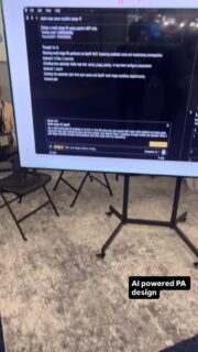
AI designing power amplifiers?
ZapRF transforms power amplifier specifications directly into a design workflow, automatically operating Keysight ADS, running simulations, and feeding the results back into its AI engine. The goal is to automate much of the repetitive design process and accelerate MMIC development.
We’re still a long way from fully automated RF design, but it’s fascinating to see how AI is pushing the boundaries in RF design.
Would you use AI to design your PA?
#IMS2026 #RF #Microwave #MMIC #PowerAmplifier
1 month ago
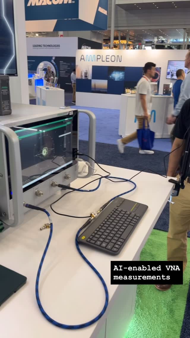
Talk to your VNA?
AI is making headway into RF test and measurement. Imagine simply talking to Anritsu’s Tensor VNA to set up complex measurements instead of navigating through cumbersome menus and settings.
And the best part? It talks back!
#IMS2026 #RF #Microwave #TestAndMeasurement #VNA AI Wireless Engineering
2 months ago
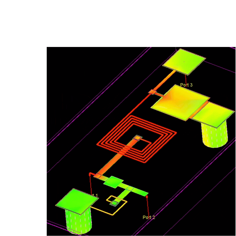
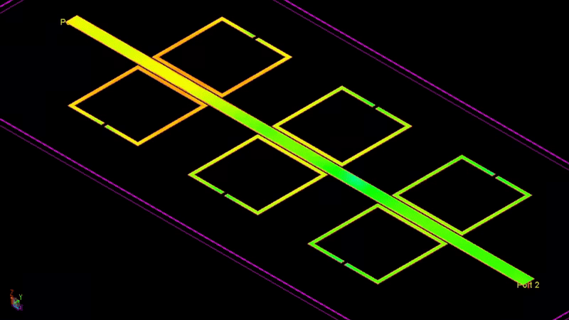
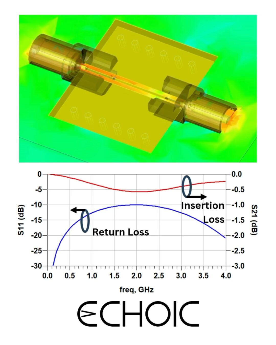
EM simulation can help RF microwave designers visualize the behavior between connector and PCB. Here, we build upon our connectors/PCB simulation to characterize the RF performance across frequency.
In the animation, we can see energy flowing from one connector through the coplanar waveguide PCB structure to the connector at the other end. This result verifies the configuration and helps us identify any anomalies (RF leakage, etc).
This analysis is performed across frequency to extract the return loss (S11) and the insertion loss (S21) of the device. A low S11 is highly desirable as it represents how much power is reflected from the incident connector and therefore how well matched it is to the signal generator. A high S21 is desirable as this represents how much loss there is across the transmission. A peak S11 of -10dB at 2GHz is acceptable but not great. A minimum S21 of -0.6dB at 2GHz is also acceptable.
EM simulations enable the designer to choose the appropriate connector design and PCB elements (trace widths, clearances, via density and placement) for high-performance, low loss connectivity.
#connectors #impedance #PCB #rfsystems #rfic #mmic
#rfengineering #rf #microwave #technology #microstrip #engineering #design #circuitdesign #circuits #em
#electromagnetics #waves
2 years ago